 20:07
20:07Original video · English narration
Original video in Russian ↗PCB fabrication using a resin printer
Conductors, solder mask, stencil, and assembly.
Watch the English version on YouTube ↗One workflow across two videos: hole plating, conductors, solder mask, stencil, and assembly.
Start with preparation ↓This guide is based on two videos by Engineer Without Experience. The techniques and explanations presented here come from the author’s original videos. The English versions below retain the original video footage, with the Russian narration replaced by AI-generated English narration.
20:07Conductors, solder mask, stencil, and assembly.
Watch the English version on YouTube ↗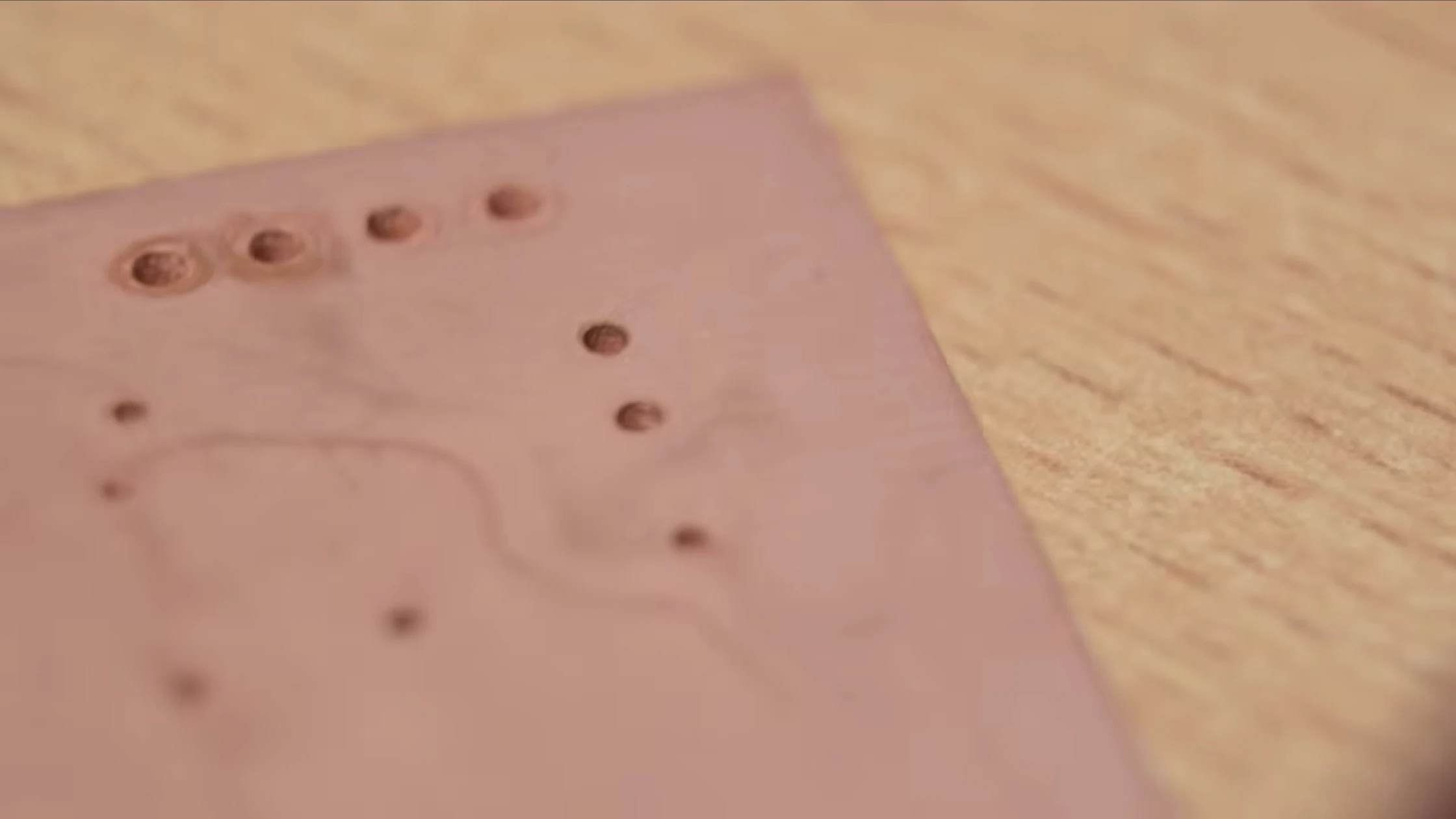 15:19
15:19Activation, electroless copper plating, and electroplating.
Watch the English version on YouTube ↗Values refer to the author's demonstrated process.
No matches. Try another word.
KiCad → STL. Alignment mark and edge clearances.
The video uses a PHOTON MONO 4 resin printer. The author gives the available working area as up to 150 × 85 mm. The exposure times below were selected for this printer.
Open the board file in the KiCad editor. Place a mark exactly halfway along the board. It is used to position the blank when exposing the second side. A mark on one layer is sufficient; it is optional for a single-sided board.
According to the author, 1 mm between the edge and the tracks or pads is sufficient for a board without solder mask. With liquid solder mask, leave at least 2 mm: trimming then removes the buildup along the edges. The author fitted the outline to a ready-cut piece of laminate, so the buildup remained on his board.
Open File → Export → STEP STL. Select STL. In the first video, the author enables the options to export the board body, cut vias in the board body, export tracks and vias, export pads, export zones, and fuse shapes. Set the output path and click Export. For a board with plated holes, the conductor exposure pattern must cover every hole; the change is shown in the second video and checked during the next file-preparation stage.
Drilled copper-clad blank → cleaning → microetching → activator → heating.
For the process shown, use a copper-clad blank with the holes already drilled, including vias. Plate the holes before creating the conductor pattern. The preparation footage shows a continuous copper surface with holes. At the end, the author also shows a test sample: he drilled the holes first and then plated them.
The first board had 140–150 holes. He tested the method with diameters starting at 0.5 mm, and with 0.7–1.6 mm holes on the second board.
The activator requires copper sulfate, sodium hypophosphite, malic acid, ammonium bifluoride NH₄HF₂, 10% ammonia solution, and distilled water. Prepare and store fluoride-containing solutions in plastic containers. The author requires extraction ventilation and personal protective equipment when handling formalin, acids, nickel salts, and ammonia.
| Component | Amount / preparation |
|---|---|
| Copper sulfate | 7 g / 20 ml warm water |
| Sodium hypophosphite | 7 g / 20 ml warm water |
| Malic acid | 3.5 g / 10 ml water |
| Ammonium bifluoride | 2.7 g / 10 ml water |
| Ammonia, 10% | 8.5 ml + 20 ml |
| Distilled water | Make up the finished activator to 100 ml |
Measure 20 ml of warm water into the first container. Add 7 g of copper sulfate. The author notes that it dissolves poorly and places the container in a water bath. Wait until it dissolves.
In a second container, dissolve 7 g of sodium hypophosphite in 20 ml of warm water. In a third container, dissolve 3.5 g of malic acid in 10 ml of water.
Dissolve 2.7 g of ammonium bifluoride in 10 ml of water in a plastic container. Measure 8.5 ml of 10% ammonia solution and pour it into this solution. The video shows the reaction during mixing. The author particularly emphasizes using plastic containers for this operation.
Let the prepared solutions cool to room temperature before mixing. Add the malic acid solution to the copper sulfate solution. Next, pour in the prepared ammonium fluoride solution, followed by the sodium hypophosphite solution. Finally, separately measure another 20 ml of 10% ammonia solution and add it to the mixture. These 20 ml are additional to the 8.5 ml used in the previous step.
Add distilled water to a total volume of 100 ml. Store the finished activator in a plastic container: the author attributes this requirement to the fluoride in the mixture.
Dissolve sodium carbonate and a surfactant in warm water. The author uses dishwasher powder, which already contains the required components. Scrub the board with a brush and rinse with distilled water.
Immerse the board in etchant for about 1 minute to lightly etch the copper and give it a matte surface. In this video, the author uses copper chloride. He also lists persulfate, ferric chloride, and citric acid with peroxide as suitable etchants. Rinse with distilled water afterward.
Immerse the board in 5% sulfuric acid for 30 seconds. Then rinse again with distilled water.
Pour the activator into a bath and immerse the board for a couple of minutes. Make sure the solution fills every hole. Remove the board and let the excess activator drain back into the bath.
Place the blank in the oven. Set the temperature to 125 °C and the time to 15 minutes. Heat the oven and start the timer. The author requires extraction ventilation and says not to inhale the fumes.
Remove the board from the oven. Rinse with distilled water and wipe with a foam sponge. Do not wash away all the black coating: compare the surface with the sample shown. Next, proceed to electroless copper plating. The author emphasizes that omitting it greatly increases the defect rate and recommends always performing this stage.
Stock solutions → solution A → add formalin immediately before use.
The author uses an alkaline formulation based on Trilon B. Its base components are copper sulfate, sodium hydroxide, Trilon B, thiourea, and formalin. He also adds nickel sulfate, sodium carbonate, and polyethylene glycol to improve the characteristics of the mixture shown.
| Component | Amount / preparation |
|---|---|
| Copper sulfate | 7.5 g |
| Trilon B | 18–20 g |
| Sodium hydroxide | 7.5 g |
| Thiourea, 1 g/l stock solution | 3 ml |
| Nickel sulfate, 10 g/100 ml solution | 10 ml |
| Sodium carbonate | 7.5 g in the preparation shown; table: 5–7.5 g |
| PEG-4000, 12 g/100 ml stock solution | 15 ml |
| Distilled water | Make up solution A to 500 ml |
| Formalin, 37%, solution B | 0.6 ml per 50 ml of solution A; add immediately before use |
This stock solution is used for both electroless and electrolytic copper plating. Take one 14 g sachet of Lavacol: according to the author, it contains 12 g of polyethylene glycol and 200 mg each of sodium chloride and potassium chloride. Add 1.2 g of table salt; the author's table gives a range of 1–1.5 g. Dissolve the contents in 80 ml of distilled water, then make up the total volume to exactly 100 ml. The video shows this recipe later, during preparation of the electroplating electrolyte; here it appears before its first use.
For the thiourea stock solution, dissolve 1 g of thiourea in 1 l of water. For the nickel sulfate additive, use the concentration of 10 g per 100 ml given in the author's table. These prepared additives will be needed when assembling solution A.
Pour about 100 ml of warm water into the first container. Dissolve 7.5 g of copper sulfate in it. Add 10 ml of the prepared nickel sulfate solution.
Pour about 100 ml of water into a second container. Dissolve 7.5 g of sodium hydroxide. Then dissolve 7.5 g of sodium carbonate. Finally, dissolve 18–20 g of Trilon B. Keep the sequence shown.
Pour the copper sulfate solution into the alkaline solution and stir. The resulting mixture should become deep blue.
Add 15 ml of the PEG stock solution and 3 ml of the thiourea stock solution. Be sure to filter the mixture. After filtering, add distilled water to a total volume of 500 ml. This is solution A.
Solution B is 37% formalin. Do not mix it with solution A in advance: the author explains that the active electroless copper solution does not last long. Measure only the amount of solution A needed for the current job.
In the demonstration, the author measures 50 ml of solution A and adds 0.6 ml of 37% formalin. Stir. The table gives the same ratio for a larger batch: 1.2 ml of formalin per 100 ml of solution A.
Immerse the activated board in the prepared solution. Cover the container with a lid and be sure to work under extraction ventilation: the author specifically mentions formalin's toxicity. Leave the board for 20–30 minutes, rocking the bath periodically. While the copper deposits, you can prepare the electroplating electrolyte.
Copper sulfate and sulfuric acid electrolyte → copper anode → controlled current → coating inspection.
The electrolyte is based on copper sulfate and sulfuric acid. The author uses polyethylene glycol as an inhibitor; the formulation also contains table salt. The table specifies battery electrolyte with a density of 1.28 g/ml. For the preparation shown, use 9 ml of the PEG stock solution prepared earlier.
| Component | Amount / preparation |
|---|---|
| Copper sulfate | 100 g |
| Initial warm water portion | 300 ml |
| Battery electrolyte, 1.28 g/ml | 400 ml (about 520 g in the author's table) |
| PEG-4000 stock solution | 9 ml in the preparation shown; table: 7–10 ml |
| Distilled water | Make up the electrolyte to 1 l |
Dissolve 100 g of copper sulfate in 300 ml of warm water. Then pour in 400 ml of battery electrolyte. Let the solution cool to room temperature.
Measure 9 ml of PEG stock solution with a syringe and add it to the electrolyte. Add distilled water to a total volume of 1 l. The author describes this solution as having high throwing power: he explains that the copper deposited inside the holes and on the flat surface has almost the same thickness.
After the immersion period, remove the board from the electroless copper solution. Rinse with distilled water. Acid-dip in 5% sulfuric acid.
Connect the positive output of the bench power supply to the copper electrode. The author uses a split and flattened copper air-conditioning tube. He explains that its phosphorus content, as in AMF anodes, helps form a black protective copper phosphide film and reduces sludge shedding into the solution. Preferably choose an anode larger than the board.
Connect the negative power-supply output directly to the PCB. The author recommends choosing a suitable container and positioning the board vertically, parallel to the anode.
In the first experiment, the board lay on the bottom: one edge was a couple of centimeters from the electrode, and the other about 10 cm away. He found no significant hole defects, but the horizontal surface collected some sludge.
Set a current density of 0.5 A per square decimeter of surface. Immerse the board in the electrolyte and deposit copper at this setting for 10–20 minutes. Use the current density stated by the author when choosing the current for your blank.
The author then increases the current density to 1–2 A/dm² to speed up the process. He explains that a layer of about 15 µm takes slightly more than an hour at 1 A/dm²; at 2 A/dm², the time is roughly halved. In the demonstration, he removes the board after an hour. These values refer to the current density being discussed, rather than a fixed current for any board area.
Remove the board and compare its surface and holes with the author's close-up images. He lightly sanded the first board to remove sludge collected on the horizontal blank and allow the photoresist to laminate evenly. On the second board, which was positioned vertically, he shows an unsanded surface without sludge.
To check the result, the author drilled and plated a separate sample, then ground the laminate edge roughly halfway through the holes. In photographs taken from the microscope screen, he estimates the copper inside the holes at about 10 µm thick. This is the demonstrated test-sample result; it should not be replaced by the estimated 15 µm from the plating-time explanation.
Photon Workshop: model position, exposure, and first layer.
After plating, prepare conductor patterns for both sides. In the new video, the author deliberately changes the pattern compared with the first video: every hole must be covered. Compare the two sides in the supplied frames. During exposure, photoresist must remain over the holes to protect the plated walls during etching. Then use the model placement, slicing, and side alignment shown in the first video.
Open the STL in ANYCUBIC PHOTON Workshop. Select the model. Go to Placing → Move and enter −1.55 mm in the Z field. This starts slicing at the copper conductors rather than the laminate body.
Open the exposure-profile settings. The author uses 40–50 seconds for the MONO 4. Enter this time in Bottom Exposure Time. In his experience, below 40 seconds, thin tracks may lift during developing; above 50 seconds, closely spaced tracks and pads may merge.
Click Slice. Move the slider on the right down to the first layer. It should show only the conductors, without a solid board body. If a white square appears, return to the model and change Z to −1.56 mm. After checking, click Save to Disk and select the printer's USB drive. For a plated board, also check that every hole is covered in the exposure patterns for both sides.
Return to the main window, select the model, and open Placing → Rotate. Click the 45° button next to Y four times for a 180° rotation. The author says to flip around the axis with the mark.
Open Edit → Clone. Enter 2 copies. Disable the main layer and move the two copies to opposite edges of the printing area. These images are used to position the ruler. Click Slice, check the first layer, and save the file to the USB drive.
A ruler on the printer screen and a shared alignment mark on the blank.
Remove the vat and moving build platform. Leave the screen's protective film in place: the author explains that it does not interfere with the process.
Select the alignment-mark file on the USB drive and start printing. Align the ruler edges with the board outline and any ruler graduation with the central KiCad mark. The author secures the ruler with ordinary adhesive tape. He mentions possible printed clips for the vat screws, but does not use them himself.
Laminate photoresist onto the already plated blank. The second video's author notes that he lightly sanded the copper surface when sludge was present to allow the film to laminate evenly. Then align and expose the conductor pattern.
Make the central mark on the blank itself with a utility knife or file. According to the author, its exact position at the center is not critical; what matters is that the mark is in the same position on both sides, without skew.
Place the blank over the screen, aligned with the ruler and mark. Expose the first side, then stop the print. Flip the blank, align the mark, and expose the second side; stop the print again. Use the bottom-layer exposure prepared earlier.
Solution sequence, rinsing, and additional UV exposure.
Dissolve 1 g of sodium carbonate in 100 ml of water. Stir the solution. The author later uses the same ratio to develop the solder mask.
Remove the polyester film from the photoresist. Immerse the blank in the stirred solution. A brush can help. The solution becomes cloudy during use; the author says it can be reused several times.
Remove the blank, rinse under running water, and dry. Give each side another 1 minute of exposure under a UV lamp. If no lamp is available, the author suggests the printer's screen test, which displays a solid UV rectangle.
For the plated board, the author of the new video uses a copper chloride solution. After exposure and developing, immerse the blank in this etchant. The photoresist covering the holes must remain intact.
In the first video, for the board without hole plating, the author used peroxide, citric acid, and a pinch of salt, mixed by eye, and turned the blank periodically. With old peroxide and no heating, etching took about 20 minutes. His explanation also described a roughly 5-minute version using fresh peroxide and hot water.
Rinse the etched board under running water. Without drying it in between, cover it with sodium hydroxide solution. The author mentions Krot drain cleaner from a hardware store. Then remove the board, rinse again under running water, and dry.
The demonstrated board shows some copper undercutting beneath the photoresist. The author attributes this to the photoresist used and considers the result acceptable. For a plated board, check the film around the holes particularly carefully before etching: in the second video, the author explains that film lifting causes the hole plating to be undercut and lose contact with the other side.
After stripping the photoresist, be sure to check continuity on every circuit. The author links open connections between sides to film lifting and etching of the plated holes. He recommends good-quality photoresist. On his board, he accepts restoring a few faulty connections with wire jumpers, comparing this with 140–150 jumpers without hole plating.
He also mentions a metal etch resist with alkaline etching as an alternative covered in another video; this sequence follows the demonstrated photoresist process.
RS-2000, mesh, and initial drying at room temperature.
The author uses RS-2000 and 120-mesh fabric. He says that 90–100 mesh is recommended for the process, but the finer 120 mesh also works for him. The frame was printed on the same printer; the author considers a metal screen-printing frame more suitable. Attach the board to the table with double-sided tape.
Mix the solder-mask components in a 3:1 ratio. The author prepares enough for both sides at once. According to his account of the datasheet, the mixed mask can be used for one day.
The author uses the printer's silicone spatula. He mentions a dedicated squeegee blade with a straight edge as the more appropriate tool. Estimate about half the prepared mixture by eye and apply it to the mesh. Press the frame down so the mesh sits tightly against the board. Spread the mask over the surface.
After application, leave the mask to dry at room temperature for 10–20 minutes. The author gives this time with reference to the datasheet. While the layer dries, he prepares the exposure pattern.
KiCad → Blender → Photon Workshop.
In KiCad, open File → Export → STEP STL. Select STL. Enable the options to export the board body, export solder mask, export pads, export zones, fuse shapes, and fill vias. Click Export. This differs from the conductor export; do not copy the entire previous set of options.
Drag the file into Blender and confirm the import with OK. Select Edit Mode at the top. To the right of the mode list, click the face-selection icon.
Click one face on the mask surface. Press Ctrl + “+” repeatedly until the entire mask surface is selected.
Select Extrude Region on the left. Drag the plus handle to extrude the volume. The author makes the layer thicker to avoid having to select precise numbers in the slicer. Repeat for the other side. The result is a board body between two solid mask layers.
In Blender, choose File → Export → STL. Open the resulting file in PHOTON Workshop. Lower the model so that slicing cuts through the mask body rather than the board body. The author chooses the position by eye.
Select the mask profile and set the time to 120 seconds. On the MASK profile screen shown, this value appears in both Normal Exposure Time and Bottom Exposure Time. Click Slice, check the first layer, and save the file to the USB drive. Flip the model 180° around Y and repeat slicing, checking, and saving for the other side.
From preliminary drying to the finished board.
The author uses the heat-press table on which he applied the coating. He sets a gap of about 1 cm between the heated surface and the table, monitors the temperature with a multimeter and thermocouple, and waits 45 minutes. The video also shows a slide of drying recommendations, reproduced separately below.
Unstick the board from the table. Start printing on the printer and check that the edge aligns with the ruler. Position the board using the previously filed mark and expose the mask.
Place the board in a container and cover it with sodium carbonate solution at the same ratio of 1 g per 100 ml of water. The author calls this a one-percent solution. He describes developing as taking just a couple of minutes. Rinse, dry, and expose under the lamp for another couple of minutes.
Repeat application, drying, alignment, exposure, and developing for the other side. The author notes a mesh-tension error after washing: the second layer was less even. He plans to cut the blank into four parts, making the unevenness less noticeable.
After developing the second side, rinse and thoroughly dry the board. The video separately shows its appearance before final drying.
Preheat the oven to about 150–160 °C. Suspend the board and dry it for 1 hour. Monitor the temperature throughout to keep it within this range. The author shows the result: the first side is smoother; the second has buildup that he says does not interfere with operation.
Compare the result with the close-up frames of the second board: the author shows the unsanded surface after vertical positioning in the electroplating bath, and holes 0.7–1.6 mm in diameter. In this sequence, the holes have already been drilled and plated before forming the conductor pattern.
KiCad → DXF → Fusion 360 → Photon Workshop.
Open the source file containing a single board instance. Disable every layer except the board outline and solder-paste layer. On the screen shown, these are Edge.Cuts and F.Paste. Enlarge the outline to a 50 × 50 mm square.
Choose File → Plot. Set the format to DXF. In the left-hand list, keep only the paste layer. In the right-hand list, specify the Edge.Cuts board outline for plotting on every layer. Select millimeters as the units and click Plot.
Open Fusion 360. Choose Insert → Insert DXF. In the right-hand panel, specify the DXF path and select a plane. When the outlines appear, position the sketch approximately in the center. The author allows using KOMPAS, Inventor, or another convenient CAD program, but demonstrates Fusion 360.
Click Inspect and measure the distance between the left inner and right outer sides of the outline. The author explains this choice by noting that the outline itself has thickness. Then click Extrude and extrude the model body.
Choose 3D Print from the File menu. Select the body to print. Fusion prepares the file and sends it to the slicer specified in the settings. This demonstrated method does not require a separate STL export.
In PHOTON Workshop, open Placing → Rotate → Rotate by Face. Select a model face to lay it flat.
Select the photoresist profile and click Slice. The author allows increasing the exposure to 100 seconds. Check the first layer and save the file to the USB drive. The frame before this change shows a profile with a 50-second exposure; do not treat it as confirmation that 100 seconds was entered.
0.1 mm stainless steel, two wires, and salt solution.
Cut a piece of 0.1 mm thick stainless steel. The author then returns to the photoresist process shown earlier: applying the pattern, exposure, and developing.
Solder two wires to the exposed part of the sheet. Tape over the back and any exposed areas on the front.
Take about half a teaspoon of ordinary table salt and add water. The author says either warm or cold water works for his method.
Connect positive to the workpiece and immerse it in the solution. For negative, the author uses a metal object such as a nail or bolt. Set the bench power supply to 0.3 A and switch it on.
The author shows that holes close to the wires etch sooner than those in the center. This is why he soldered two wires: one wire would make the difference more noticeable. He also explains that positioning a wire on the side with larger holes may increase edge undercutting beneath the photoresist and increase the paste quantity on large pads. This is his explanation, not a mandatory extra step.
When the hole outlines become clearly visible from the back, switch off the power supply. Remove the stencil, rinse, dry, and desolder the wires. Remove any remaining burrs.
Securing the stencil, placing components, and the final result.
Use double-sided tape to attach a piece of laminate to a wooden board: the stencil will rest against it. Attach the PCB beside it. Align the stencil openings with the PCB pads.
The author uses a second piece of stainless steel as a spatula. Apply paste at the edge and spread it, pressing it into the stencil openings. The frames show the paste deposited on the pads.
Place the components onto the paste-covered pads. The video shows this stage in assembly footage.
Set the hot-air tool to 300 °C and reflow the solder. After the author signs off, the video shows soldering, work with tweezers, and photographs of the finished board.
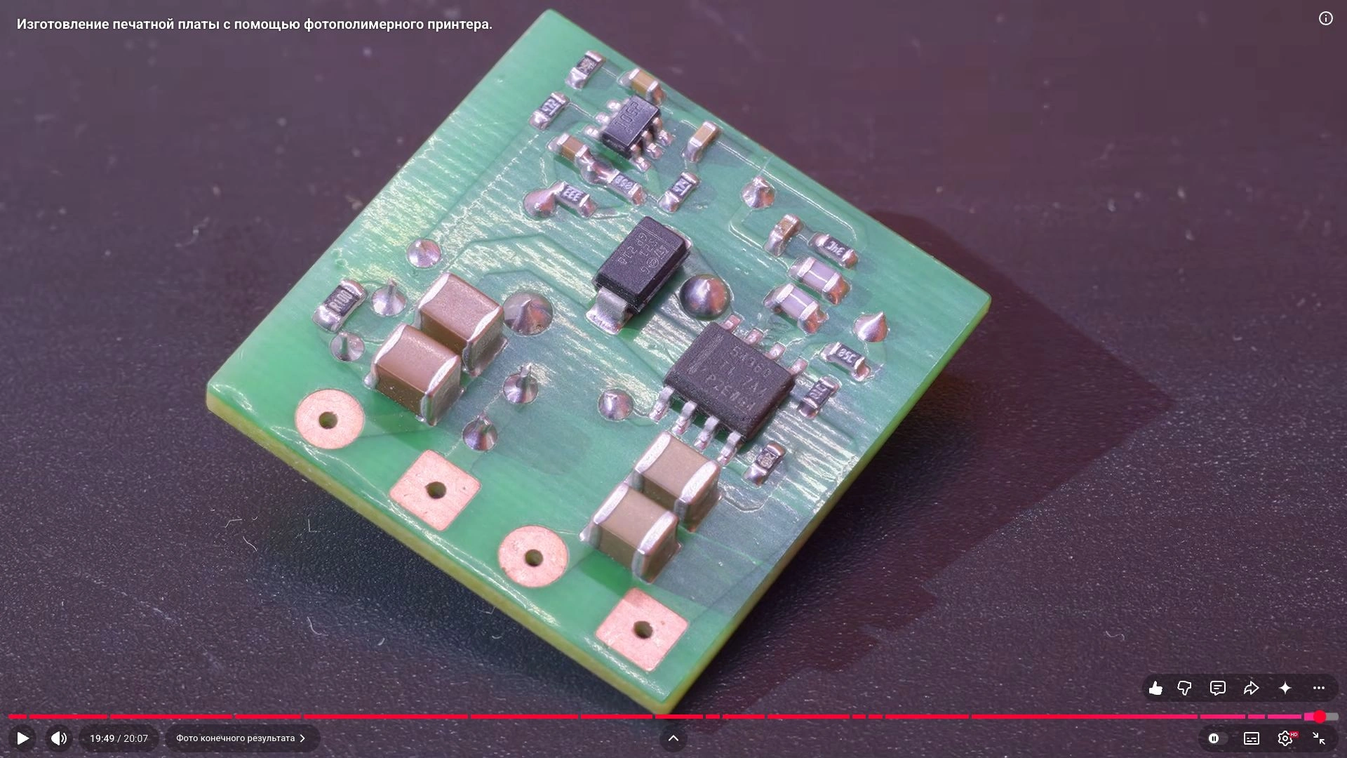
The final photographs show the board after assembly. The video ends at about 20:07.
The author shows a couple of holes on the second board under a microscope after soldering. Compare their appearance with the frame. These images were photographed from the microscope screen.